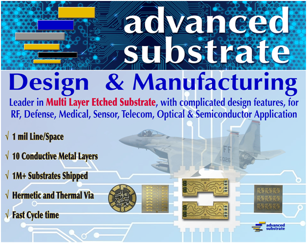
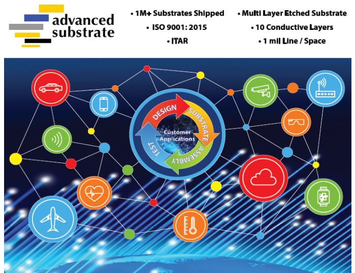
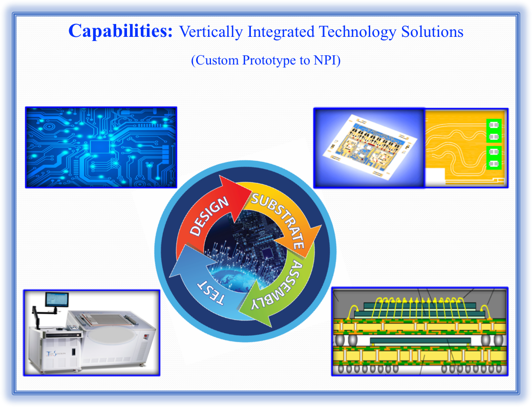
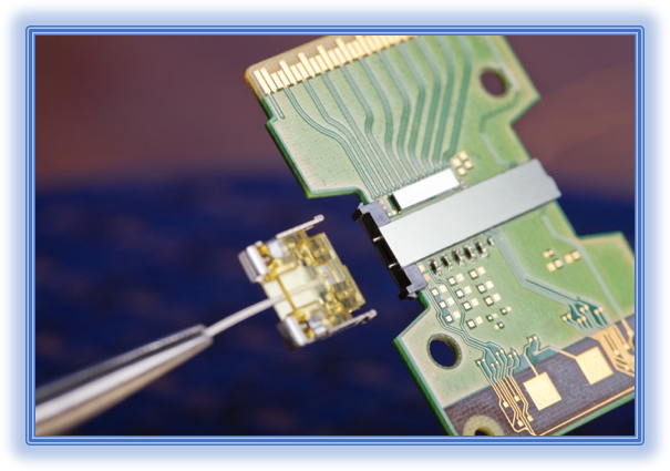
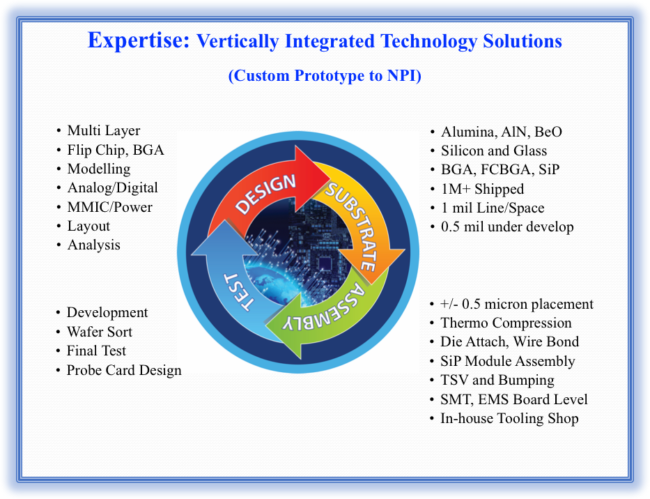
Advanced Substrate specializes in providing vertically integrated solutions for sophisticated and unique microelectronics packaging requirements in: Silicon Photonics, Chip on Board Packages for Medical, Defense, IoT Sensors, Telecom, Driverless Car LiDAR and Commercial applications.
Advanced Substrate has built a solid reputation for quality, craftsmanship and expertise in providing the most advanced and innovative packaging solutions.
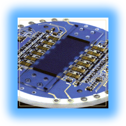
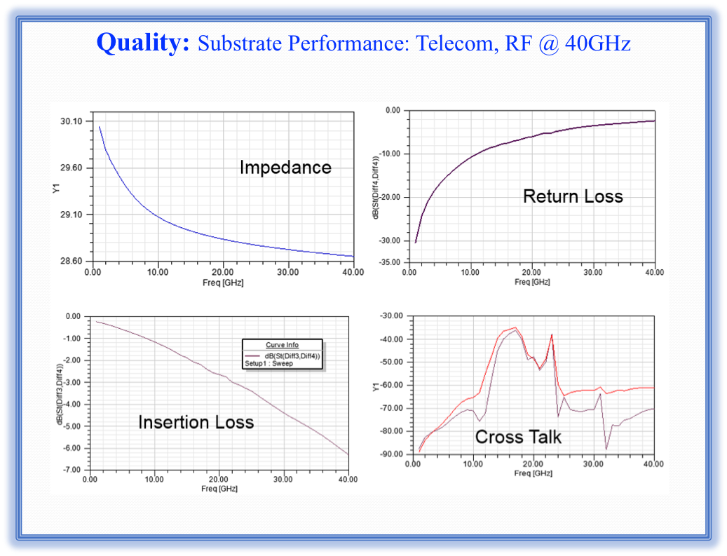
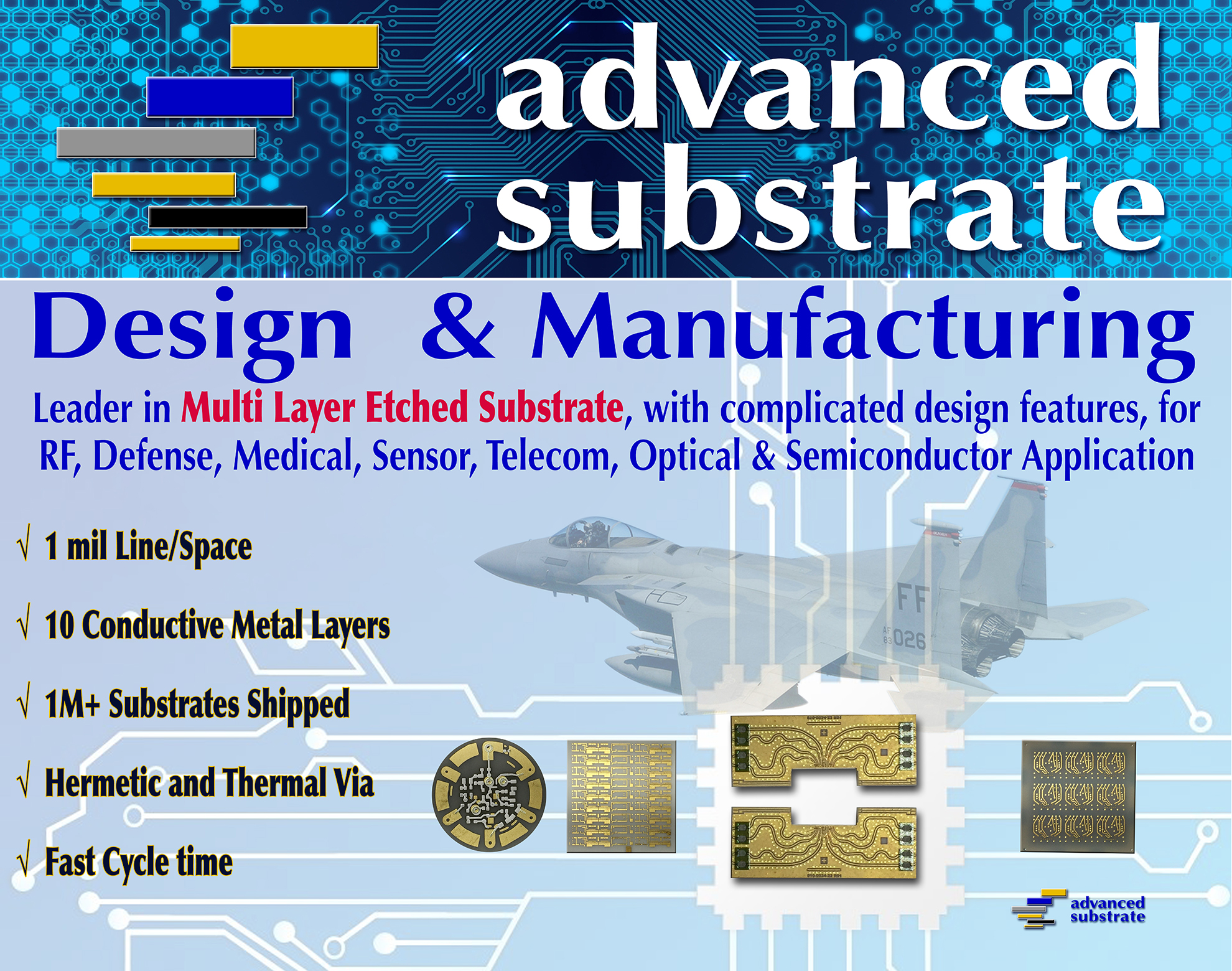
The applications in LiDAR, Silicon Photonics, 400G Telecom, 40GHz+ RF Wireless, Cloud Computing, Innovative X-ray, Carbon Sensors and others have created a new era of printed circuit board (PCB) design transformation to system in package (SiP) design methodology. The need for SiP solutions has driven the entire semiconductor, packaging, design chain and supply chain industries to develop advanced technologies that can address the increasing needs for cost reduction, size reduction and performance enhancements for advanced electronic systems.
The transition to SiP design requires new thinking, new approaches and solid understanding of assembly, electronic circuit designs, components integration and final testing as well as functional verifications. PCB will have technological and pricing issues to meet challenges of next generation in: component placement with sufficient distance to minimize electromagnetic coupling among passive components, pre-packaged Integrated Circuits, highly capacitive interconnect structures, and relatively easy to modify and enhance circuits. To address these challenges, Advanced Substrate team provides value add engineering services by using their 100+ years of domain experience.
SUBSTRATE DESIGN
Advanced Substrate co-works with customer to design and define the electrical and mechanical requirement of the products. Advanced Substrate is dedicated to design and manufacture substrate of high reliability applications. In order to help with time to market, our team discuss to understand end application and special design requirement; such as, component size, placement, interference, impedance, circuit routing, thermal constraints, environmental constraints, etc. Advanced Substrate has the knowledge, experience and resources to handle complicated design requirements in order to provide the best possible product the first time.
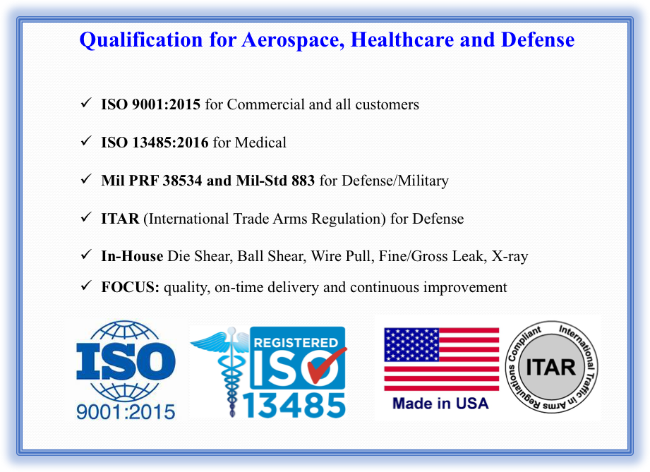
We are reliable supplier of high reliability substrates to the aerospace, automotive, wireless, defense, industrial and medical applications. We can design the substrate by following customer’s net-list along with design guideline.
THICK FILM SUBSTRATE
Advanced Substrate’s talented and experienced technical team has 100+ years of hands on experience to support your thick film substrate requirements.
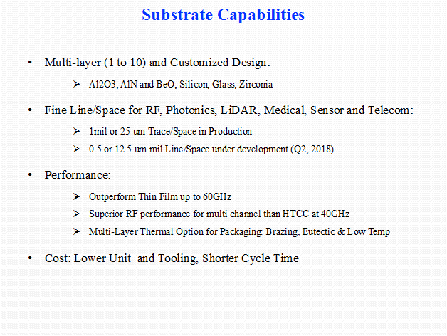
Typical Ceramic Substrates:: 96% and 99% Alumina, Polished, Lapped, AlN, BeO, Silicon Wafer. We typically keep stock of 0.010", 0.015”, 0.025", and 0.30" thick Alumina plates. This allows us to laser scribe substrates and turn your orders quickly.
We typically keep stock of 0.010", 0.015”, 0.025", and 0.30" thick Alumina plates. This allows us to laser scribe substrates and turn your orders quickly.
Advanced Substrate Offers:
- Design Services (from process reviews to full layout support)
- Multi-Layer Printing (up to 10 conductive layers, 80+ prints)
- Through hole printing (plugged and plated)
- Double sided printing
- Resistor Printing and Trimming (5-6 decades possible)
- Thermister Printing and Trimming
- 1.0 mil lines/spaces
- Hermetic Via
- Vacuum stage for front to back pull through
ETCH THICK FILM
For critical application, tighter line spacing is a necessity which can be resolved by using ETF (Etched Thick Film). Advanced Substrate offers partial or complete etching solutions. ETF can reduce line widths to 0.001". For RF and digital applications, etched thick film has proven a cost effective alternative to thin film circuits, with shorter lead time.
Advanced Substrate Offers:
- Etch Thick Film (down to 1 mil lines and spaces)
- Fodel © Printing
- Edge Transition Technology (fine lines wraped around 90 degree edge of ceramic)
- Diffusion patterning to produce via resolutions down to 0.004"
- Solid thru metallized vias
- 14,000 via filled per 13” wafer with 99.99% via continuity and isolation yield
LASER CUTTING
Advanced Substrate has in-house laser cutting and substrate profiling facility that can be used to produce double-sided substrates via through-hole. These types of substrates offer significant space saving in terms of circuit size and density as well asalso deliver superior technical performance. Advanced Substrate keeps standard thickness Alumina panels (96% Alumina, 99.6% Al2O3, etc) in stock. This allows us to make physical samples of complex designs the same day that we receive CAD data. Advanced Substrate also offers ceramic laser scribing on a stand alone basis for outside customers.
RESISTOR TRIMMING
Advanced Substrate has in-house YAG laser system to trim resistors and thermistors. This laser, combined with our Probe Card Assembly and Planarization Stations, give us a complete system to trim your product with competitive cost advantage and better cycle time.
To test the integrity of interconnecting layers, we use dedicated test equipment that can measure point-to-point circuit resistance or net capacitance to ensure that a substrate is fully operational before it is populated with components. The laser trimming equipment allows Advanced Substrate to precisely adjust and trim resistors to meet preset design tolerances.
We have trimmed from 100 mOhms to 1 GOhms. The tolerances achievable depend upon the resistance value and the geometry of the resistor. Although this capability is mainly used to support internal demand, we will gladly provide this service to outside customers as well.
Advanced Substrate Offers:
- Ratio Trimming
- Match Trimming
- Loop Trimming
- Metal Trimming
- Comparator Trimming
- Custom Trim Protocols for Customer Specific Applications
ASSEMBLY